Research at the Laboratory of Crystallography
Commensurate charge-density wave in SmNiC2 at T = 60 K rendered incommensurate by frustration
SmNiC2 crystallizes at room temperature in the orthorhombic CeNiC2 structure type and is isostructural to other RNiC2 compounds (R = rare earth metal). Upon lowering the temperature it undergoes two phase-transitions. Below TCDW = 148 K a charge-density-wave (CDW) state is formed, which is destroyed by a second phase transition at a temperature TC = 17.7 K to a ferromagnetic (FM) state [1].
At the Laboratory of Crystallography we have done single crystal X-ray diffraction with synchrotron X-ray radiation at Hasylab in Hamburg, and found the lattice of SmNiC2 to remain orthorhombic in both the CDW- and the FM-phase. This finding has implications for the allowed structural distortions at low temperature.
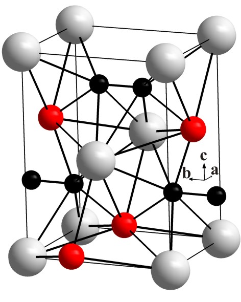
Figure 1: Basic crystal structure of SmNiC2.
A data collection of main and satellite reflections at T = 60 K has determined the modulated structure in the CDW-phase by use of the superspace approach [2]. The structure of SmNiC2 is built of layers of Ni and Sm atoms stacked along the c axis, the C atoms are located as C2 between these layers. Ni atoms form dimerized chains along the a axis and show the largest modulation amplitude as well as the the largest variation in bonding distances between neighbouring atoms. For that reason, the Ni atoms carry the valence band responsible for the CDW. This observation is affirmed by the electronic resistivity, which is lowest along the a axis [1]. In one layer, neighbouring Ni chains have an anti-phase relation. For a single layer, the optimal modulation wave vector would be commensurate (0.5, 0.5, 0).
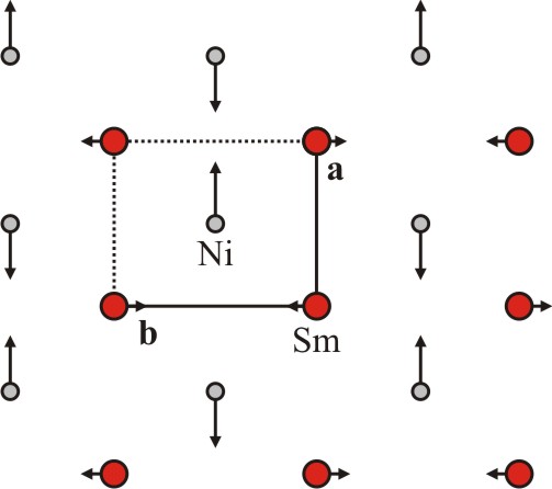
Figure 2: One layer of Sm and Ni atoms with atomic displacements indicated by arrows.
The relation between chains in neighbouring layers is given by the A center. In the case of this commensurate modulation wave vector, atoms modulated in one layer would, therefore, have zero modulation in the next layers . Due to the identical environments, this is implausible. Instead of this, the A center provides a frustration between the chains in neighbouring layers, which leads to an incommensurate coupling between the layers. In consequence, the modulation wave vector for the whole structure is qCDW = (0.5, 0.516, 0) [3].
Participating researchers at the Laboratory of Crystallography in Bayreuth: Alexander Wölfel, Liang Li and Sander van Smaalen. The research has been done in collaboration with Susumu Shimomura (Department of Physics, Kyoto Sangyo University, Kyoto, Japan) and Hideya Onodera (Department of Physics, Tohoku University, Sendai, Japan).
Literature:
[1] S. Shimomura, C. Hayashi, G. Asaka, N. Wakabayashi, M. Mizumaki, and H. Onodera: Charge- Density-Wave Destruction and Ferromagnetic Order in SmNiC2; Phys. Rev. Lett. 102, 076404, (2009).
[2] S. van Smaalen; Incommensurate Crystallography (Oxford University Press, Oxford, 2007).
[3] A.Wölfel, L. Li, S. Shimomura, H. Onodera, and S. van Smaalen: Commensurate charge-density wave with frustrated interchain coupling in SmNiC2; Phys. Rev. B 82, 054120, (2010).